The Science Behind Scratch Resistance Evaluation
New 14 11 月, 2025
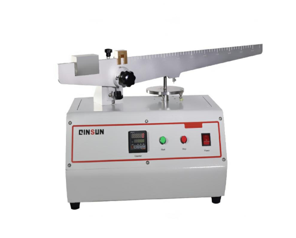
Scratch testing represents one of the most sophisticated methodologies in material surface characterization, providing crucial insights into how materials behave under mechanical stress. This scientific approach simulates real-world scratching scenarios through controlled laboratory conditions, enabling researchers and engineers to quantify material resistance with exceptional precision. The fundamental principle involves dragging a precisely calibrated stylus across a material surface under predetermined normal loads, while monitoring the interaction between the stylus and specimen in real-time. This process generates valuable data about material performance that directly correlates to actual usage conditions.
The instrumentation employs three distinct detection methodologies, each offering unique advantages for specific applications. The conductive detection method operates on the principle of electrical continuity, where a constant electrical potential is maintained between the stylus and substrate. When the stylus penetrates through a non-conductive coating and reaches the conductive base material, the resulting change in electrical resistance triggers detection circuits. This method proves particularly effective for quality control of protective coatings in electronic devices and automotive components. The optical detection system utilizes high-resolution digital microscopy combined with advanced image processing algorithms to analyze scratch morphology. Modern systems can achieve resolution down to 0.1 micrometers, allowing for detailed examination of plastic deformation, cracking patterns, and material pile-up along scratch edges. The acoustic emission methodology captures high-frequency stress waves generated by material deformation and fracture events. These acoustic signals, typically ranging from 100 kHz to 1 MHz, provide real-time information about sub-surface damage initiation and propagation that would otherwise remain invisible to optical inspection.
Contemporary scratch testing instruments incorporate sophisticated automation features that significantly enhance testing efficiency and reproducibility. The integrated control systems manage all critical parameters including loading force, scratching speed, and stylus positioning with micron-level precision. Advanced memory functions allow storage of multiple testing protocols, enabling laboratories to maintain standardized procedures across different operators and testing sessions. Safety mechanisms include automatic stylus retraction systems that prevent secondary damage during return cycles, and intelligent monitoring systems that can detect abnormal testing conditions through real-time data analysis. The modular design philosophy enables seamless integration of specialized components, such as environmental chambers for temperature-controlled testing, or nano-indentation modules for thin-film characterization.
The applications of scratch testing span across multiple industries and research domains. In automotive manufacturing, it ensures the durability of interior components like polymer dashboards and coated metallic surfaces against everyday wear. The aerospace industry relies on scratch testing to validate thermal barrier coatings and composite materials that must withstand extreme environmental conditions. Consumer electronics manufacturers utilize these tests to verify the scratch resistance of device housings and display panels, directly impacting product longevity and customer satisfaction. Research institutions employ scratch testing for fundamental studies in tribology and surface science, while certification bodies use it to verify compliance with international standards. The educational value of scratch testing extends to engineering curricula, where it serves as a practical demonstration of material behavior principles and quality control methodologies.